
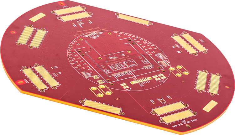
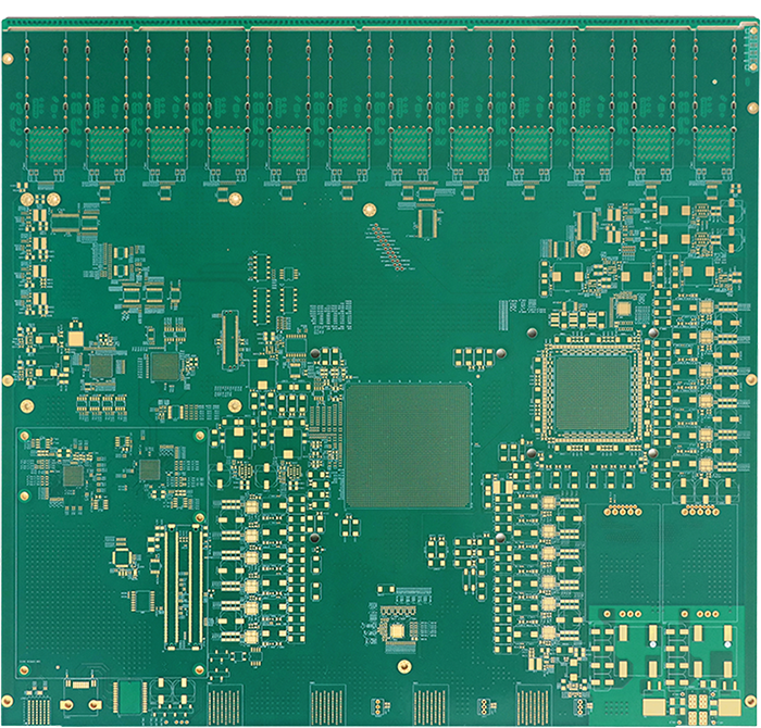
▪ Number of layers – 34L
▪ Material - S1000-2
▪ Plate thickness —— 4.6mm
▪ Aspect ratio – 18:1
▪ Blind holes – L32 – L34
▪ Inner layer copper thickness – 1 & 2 oz
▪ Minimum line width/line spacing - 0.1mm
▪ Minimum hole diameter - 0.25/0.4mm
▪ Impedance - more than 20 impedance lines
▪ Surface treatment - immersion gold
")
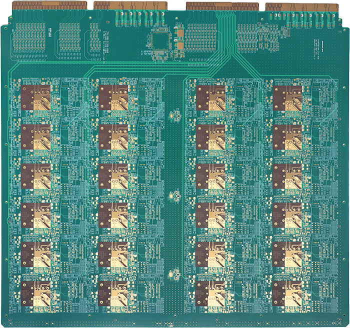
▪ Number of layers - 20L
▪ Material - IT180ATC
▪ Plate thickness —— 2.35±0.1mm
▪Copper thickness of inner and outer layers——0.5OZ
▪ Minimum line width/line spacing - 0.072/0.255mm
▪ Minimum hole diameter - 0.131mm
▪ Surface treatment - immersed gold + gold finger
▪ Application areas - communication equipment
")
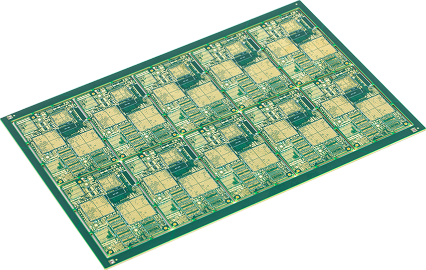
▪ Number of layers – 22L
▪ Material - FR-4(Tg180) VT-47
▪ Plate thickness —— 2.59+/-0.26mm
▪ Minimum line width/space - 3.5/5.0mil
▪ Minimum hole diameter - 0.25mm
▪ Surface treatment - immersion gold

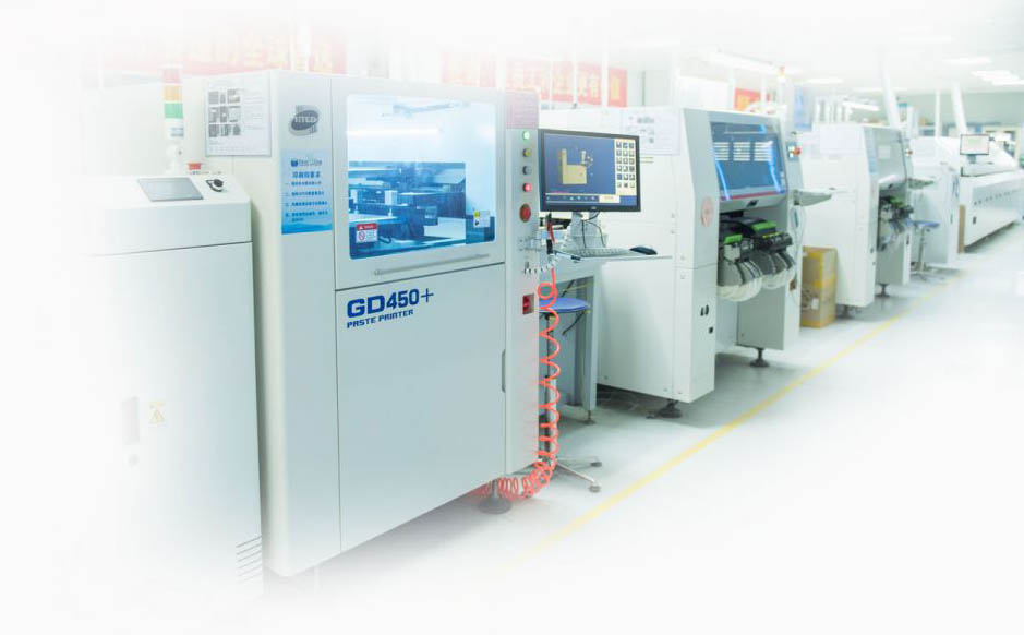
SMT: Can mount 0201 devices, 0.3 BGA and 0.4 connectors.
Wave: pluggable wave soldering assembly and burning test
Testing: LCR instrument, AOI, X-RAY to ensure welding quality
▪ Can be used in empty slots or on top and bottom of PCB
▪ Available for through-hole connections
▪ Number of floors – 4 floors
▪ Material - S1000-2M
▪ Plate thickness - 2.0 mm
▪ Lamination - buried copper blocks
▪ Blind vias - 1-2 layers
▪ Minimum line width/line spacing - 0.2mm
▪ Surface treatment - immersed tin
▪ Application areas – Thermal control solutions
")
Number of layers - 10 L
▪HDI(2+N+2)
▪Microporous structure——L1-L2, L2-L3, L8-L9, L9-L10
▪Buried via——L3-L8
▪Minimum pad size——3.0milx3.0mil
▪Minimum pad spacing - 2.5mil
▪Surface treatment - nickel-palladium
")
▪ Number of layers: 12L
▪ Product model——4 QSFP-DD
▪ Material – M6 (R-5775)
▪ Finished product thickness tolerance - gold finger area 1.2±0.01mm
▪ Plug shape tolerance ——± 0.05mm
▪ Hole filling recess——<16μm
▪ Surface treatment - nickel-palladium + electroplated hard gold
▪ Thermal design - embedded copper block
")
▪ Number of layers – 8L
▪ Material - DS7409-HGB
▪ Plate thickness —— 0.7mm
▪ Copper thickness of inner and outer layers —— H/H oz
▪ Minimum line width/line spacing - 0.05/0.05mm
▪ Minimum hole diameter - 0.1mm
▪ Surface treatment - Nickel Palladium
")
Features:
▪ Number of layers - 2 Layer
▪ Material – Ceramic Aluminum Nitride
▪ Plate thickness —— 0.38 +/-0.03mm
▪ Line width and line spacing - 4/4mil
▪ Application fields - automobile, Led
▪ High stability, low dielectric constant
▪ High thermal conductivity - ≥24W/M·K
▪ High breakdown voltage —— ≥15KV/mm
▪ Low CTE - about 6.7~7.8ppm/K
Features:
▪ Number of layers - 1 layer
▪ Material - high alumina glass
▪ Plate thickness —— 1.0 +/-0.1mm
▪ Line width and line spacing - 4/4mil
▪ Application areas - Led
▪ High breakdown voltage —— ≥15KV/mm
▪ Low CTE - about 9.9ppm/K
▪ Low dielectric constant
▪ Number of layers – 12L
▪ Material - EM-827
▪ Plate thickness —— 5.0mm
▪ Inner and outer copper thickness - 4 oz
▪ Minimum line width/line spacing - 0.45/0.30mm
▪ Minimum hole diameter - 0.4mm
▪ Surface treatment - immersion gold
")
▪ Number of layers – 4L
▪ Material - S1000-2M
▪ Plate thickness - 2.5 mm
▪ Surface treatment - immersed tin
▪ Others - ferrite shielding, high magnetic permeability
")
▪ Industrial control system
▪ Number of layers – 12L
▪ Material - EM370(Z)
▪ Plate thickness —— 3.0mm
▪ Copper thickness of inner and outer layers—— 6 OZ(RTF)
▪ Minimum line width/line spacing - 0.38/0.25mm
▪ Minimum hole diameter - 0.3mm
▪ Surface treatment - immersed gold 3U”
")
▪ Number of floors – 8 floors
▪ Material - TU768
▪ Plate thickness - 3.2mm
▪ Copper thickness of inner and outer layers —— 4OZ
▪ Minimum line width/line spacing - 0.3/0.3mm
▪ Minimum hole diameter - 0.7mm
▪ Surface treatment - immersed gold 2U"
▪ Application areas - Sightseeing equipment
")
▪ Number of layers – 14L
▪ Material - S1000-2M
▪ Plate thickness —— 2.55mm
▪Inner layer copper thickness——3OZ
▪ Outer layer copper thickness —— 3OZum
▪ Minimum line width/line spacing - 0.26mm/0.28mm
▪ Minimum hole diameter - 0.6mm
▪ Surface treatment - immersed gold 2U"
")
▪ Number of layers - 10L
▪ Material - high TG FR-4+PI base material
▪ Plate thickness —— 1.2±0.12mm
▪ Minimum line width/line spacing - 0.076/0.076mm
▪ Minimum hole diameter - 0.15mm
▪ Surface treatment - immersion gold
")
▪ Number of layers - 16L
▪ Material – High TG FR-4 + Flex
▪ Plate thickness —— 1.7±0.17mm
▪ Minimum line width/line spacing - 0.09/0.08mm
▪ Minimum hole diameter - 0.15mm
▪ Surface treatment - immersion gold
")
▪ Number of layers – 2L
▪ Material - Doosan DS-7409DV high frequency material
▪ Plate thickness——0.76mm±0.07mm
▪ Minimum line width/line spacing - 0.580mm±5%
▪ Minimum hole diameter - 0.2mm
▪ Surface treatment - immersed tin
")
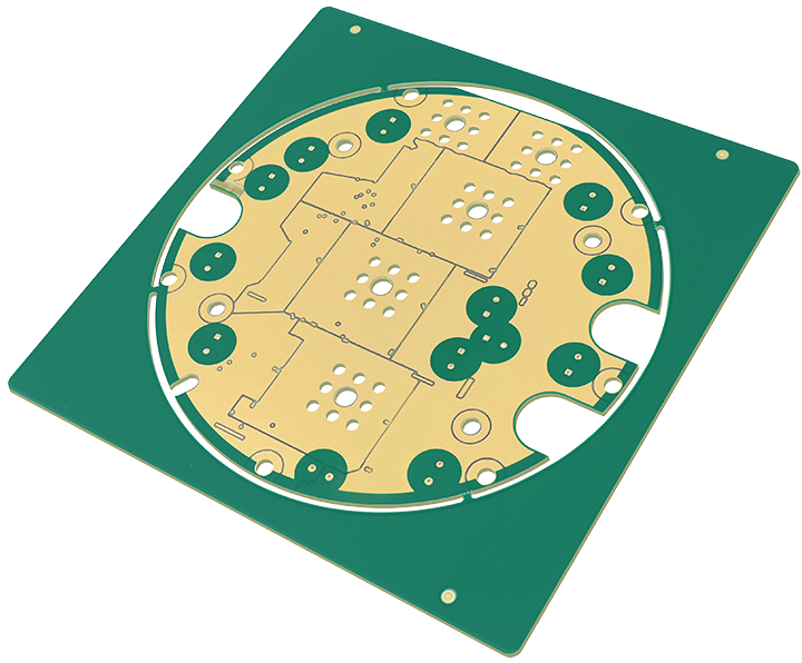
▪ 22L
▪ High speed and low consumption
▪ 2 times of lamination (3-22 layers for the first time, 1-22 layers for the second time)
▪ 11 back drill belts, VIPPO
▪ Embedded with 22 copper blocks
▪ 10 different impedances (single-ended/differential)
▪ High voltage and low voltage electroplating hole filling process
")
▪ Number of layers – 8L
▪ Material – MT77
▪ Plate thickness——1.43mm
▪ Copper thickness of inner and outer layers——1oz
▪ Minimum line width/line spacing - 0.25/0.25mm
▪ Minimum hole diameter - 0.3mm
▪ Surface treatment - immersion gold
▪ Others - 0.127mm back drilling
")
▪ Number of layers – 26L
▪ Material – Tachyon 100G, hydrocarbon
▪ Plate thickness —— 3.5±0.35mm
▪ Copper thickness of inner and outer layers —— 0.33OZ
▪ Minimum line width/line spacing - 0.118/0.051mm
▪ Minimum hole diameter - 0.225mm
▪ Surface treatment - immersion gold
▪ Application areas - industrial control systems
")