
▪ Can be used in empty slots or on top and bottom of PCB
▪ Available for through-hole connections
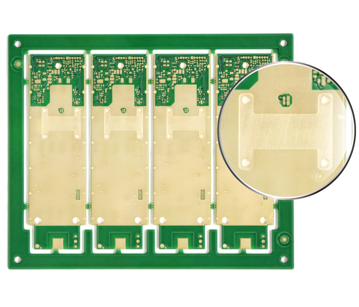
▪ Number of floors – 4 floors
▪ Material - S1000-2M
▪ Plate thickness - 2.0 mm
▪ Lamination - buried copper blocks
▪ Blind vias - 1-2 layers
▪ Minimum line width/line spacing - 0.2mm
▪ Surface treatment - immersed tin
▪ Application areas – Thermal control solutions
")
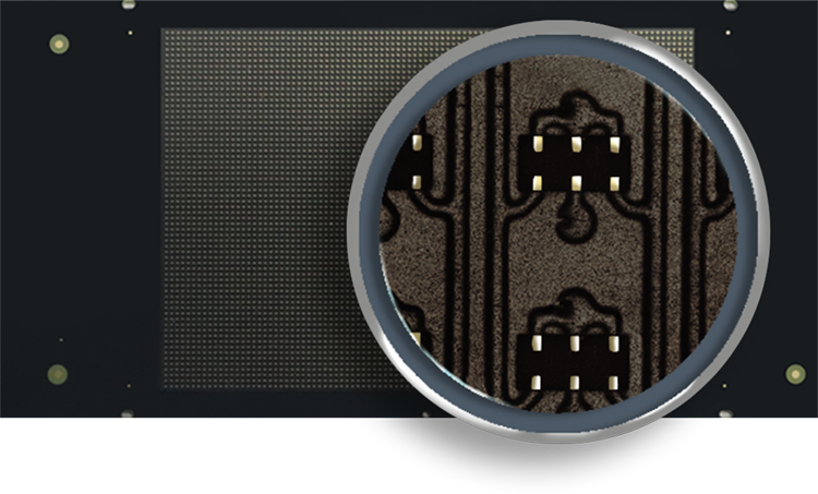
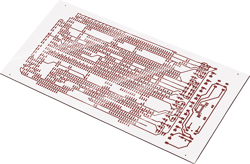
Number of layers - 10 L
▪HDI(2+N+2)
▪Microporous structure——L1-L2, L2-L3, L8-L9, L9-L10
▪Buried via——L3-L8
▪Minimum pad size——3.0milx3.0mil
▪Minimum pad spacing - 2.5mil
▪Surface treatment - nickel-palladium
")
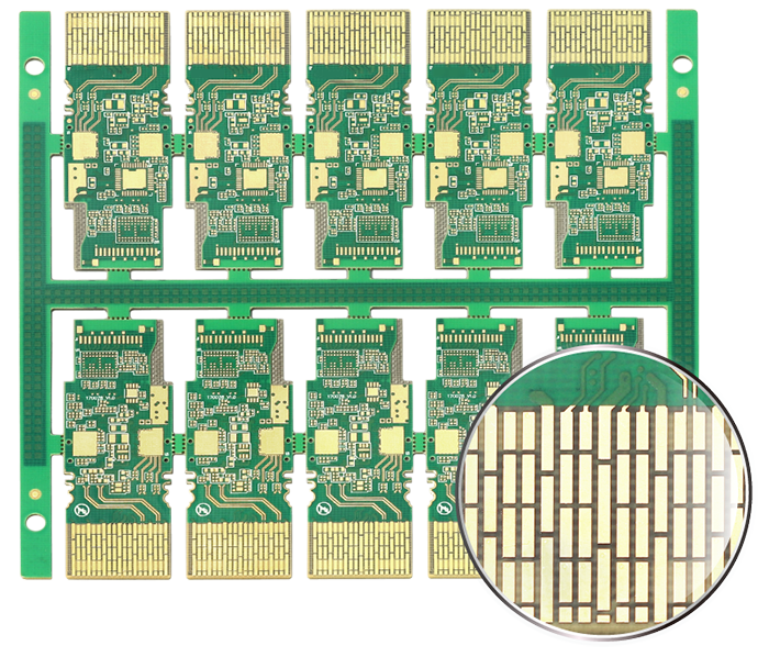
▪ Number of layers: 12L
▪ Product model——4 QSFP-DD
▪ Material – M6 (R-5775)
▪ Finished product thickness tolerance - gold finger area 1.2±0.01mm
▪ Plug shape tolerance ——± 0.05mm
▪ Hole filling recess——<16μm
▪ Surface treatment - nickel-palladium + electroplated hard gold
▪ Thermal design - embedded copper block
")
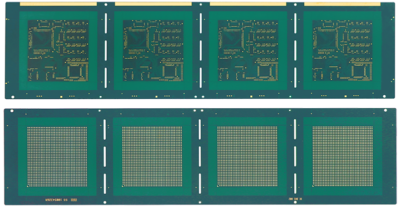
▪ Number of layers – 8L
▪ Material - DS7409-HGB
▪ Plate thickness —— 0.7mm
▪ Copper thickness of inner and outer layers —— H/H oz
▪ Minimum line width/line spacing - 0.05/0.05mm
▪ Minimum hole diameter - 0.1mm
▪ Surface treatment - Nickel Palladium
")
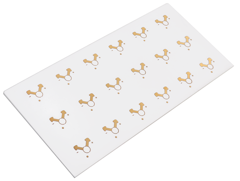
Features:
▪ Number of layers - 2 Layer
▪ Material – Ceramic Aluminum Nitride
▪ Plate thickness —— 0.38 +/-0.03mm
▪ Line width and line spacing - 4/4mil
▪ Application fields - automobile, Led
▪ High stability, low dielectric constant
▪ High thermal conductivity - ≥24W/M·K
▪ High breakdown voltage —— ≥15KV/mm
▪ Low CTE - about 6.7~7.8ppm/K
Features:
▪ Number of layers - 1 layer
▪ Material - high alumina glass
▪ Plate thickness —— 1.0 +/-0.1mm
▪ Line width and line spacing - 4/4mil
▪ Application areas - Led
▪ High breakdown voltage —— ≥15KV/mm
▪ Low CTE - about 9.9ppm/K
▪ Low dielectric constant